The C4S stands for "Camille Cascode Constant Current Source." It was designed by Buddha (John Camille). This current source is simple, robust and in my opinion functions very well. Bottlehead sells the C4S as a kit. With this web page I hope to show you how to take this kit and get more out of it.
There are a couple critical items to watch on the output transistor:
1.0 Temperature: Keep the junction below 100 C
and try to keep the heatsink below 60 C in normal operation.
1.1 Temperature: Keep the junction below 150
C during faults
2. SOA (Safe operating area)
3. Current gain.
The specification sheet on the MJE350 says you can get 20W out of the part. This can only happen if you let the junction rise to 150 C and you use a water cooled heatsink to keep the metal portion of the case at 25 C. ( Marketing is Marketing. The "model" sitting in the car does not come with the car. [You probably don't really want the baggage that comes with that "model" anyway.] )
Thermal Issues with the Transistor.
First edition 02/10/01 Last Update 02/22/01
First lets assume that the air around the C4S is running about 40 C ( 104 F ) and everything is working normally. Next lets limit the heatsink rise to 60 C. Lastly for reliability, we want to keep the junction below 100 C (105 C is also OK, 120 C is too darn hot!) Keeping the heatsink below 60 C is to keep from burning your fingers if you accidentally touch the heatsink right AFTER you turn the power off and bleed the capacitors down.
Finally lets assume the 115V is at high line (127 V AC), the tube is shorted and the ambient temperature is 40 C. Under these conditions we will keep the junction temperature below 150 C (manufacture's rated.)
Condition 1, the MJE350 with no heatsink:
The bare MJE350 is 84 C/ W (standing upright so that you can't
balance a marble in the hole through the part).
The MJE350 is 6.25 C/W junction to case.
For a 60 C surface temperature on the MJE350:
(60 C - 40 C)/ (84 C/ W - 6.25) = 20 C/ 78 C/ W = 0.256 WFor a 100 C junction temperature:
Note: Subtract rise from Rjc (6.25 C/ W) from Rja (84 C/ W) to get case temperature.
(100 C - 40 C)/ 84 C/ W = 60 C/ 84 C/ W = 0.714 WFor a 150 C junction temperature:
This is no where near 20W.
(150 C - 40 C)/ 84 C/ W = 1.31 W with no extra heatsinking and running the junction way too hot for normal operation.Condition 2, the MJE350 with a small heatsink:
The MJE350 is 6.25 C/W junction to case.
I estimate a TO-220 Berg K10 insulator with a
0.125 dia hole used on a TO-255AA will be 3.75 C/W.
The heavy duty radio shack TO-220 heatsink is
20 C/W (the one with multiple fins.)
For a 60 C surface temperature of the heatsink:
(60 C - 40 C)/20 C/W = 1 W max.For a 100 C junction temperature with the heatsink and transistor under normal operating conditions:
(100 C - 40 C)/(6.25 + 3.75 + 20 C/W) = 60/30 = 2.0 W max.For a 150 C junction temperature with the heatsink and transistor under fault conditions:
(150 C - 40 C)/(6.25 + 3.75 + 20 C/W) = 110/30 = 3.6 W max.* If you don't mind burning your fingers with the power off and nothing meltable is near the C4S: use 2 W for maximum normal operating conditions.
1 W/ 100 V = 10 mA
1 W/ 150 V = 6.7 mA
2 W/ 100 V = 20.0 mA
or 2 W/ 20.0 mA = 100 V
2 W/ 150 V = 13.3 mA
or 2 W/ 13.3 mA = 150 V
3.6 W/ 200 V = 18 mA or 3.6
W/ 18 mA = 200 V
3.6 W/ 300 V = 12 mA or
3.6 W/ 12 mA = 300 V *** Note 1
*** Note 1: 300 V at 12 mA violates the SOA of the
MJE350 if this condition exists for more than ~0.1 second! ***
In a future discussion below, we will be using the C4S at 7.5 mA with a fault voltage of 300V. Let's calculate the junction temperature under these conditions with this small heatsink attached:
300V * 7.5 mA = 2.25 W.Here are a few heatsinks picked from the Digikey Catalog sort of at random. There are hundreds of heatsinks you can use out there. I am not recommending nor discouraging the use of any of these part numbers. They were just picked so I can give you an example.
2.25W * 30 C/W + 40 C ambient = 67.5 C rise + 40 C = 108 C (OK)
We will still have to check normal operating conditions, because they could be worse than the fault condition.
When you go to places like AAVID to look at heatsinks (click the search button on their first page), you will notice that the C/W varies with power. This is because the hotter the heatsink is, the better it works. (At least some things work in our favor.) Make sure you use the C/W for the power loss you have and not the advertised C/W.
An important land mark is that for a 100 C junction and an infinite heatsink, we can only put 6 watts into the MJE350.
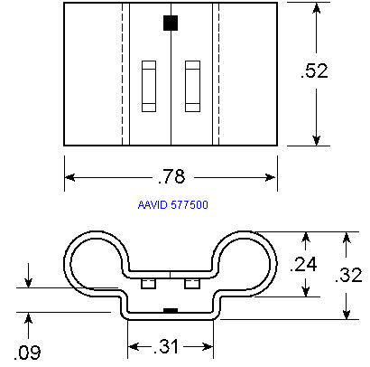
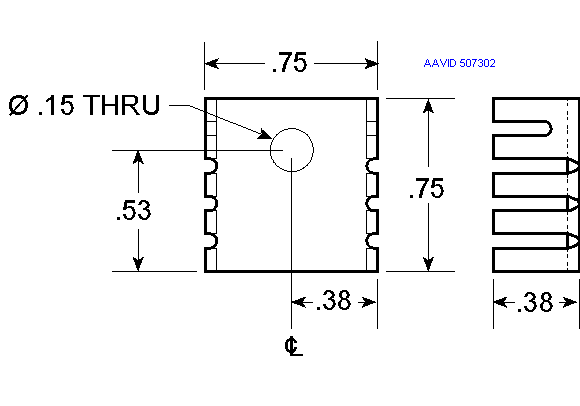
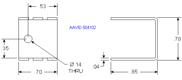
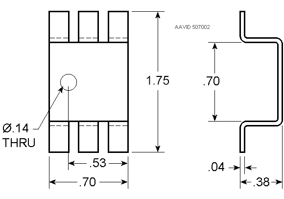
| AAVID
P/N |
10 pc
cost each (Digikey) |
Height (in) | Width (in) | Depth (in) | C/W at
2 W |
Notes | 150 C
MJE350 junction Watts |
100 C
MJE350 junction Watts |
60 C
heatsink surface watts |
| Bare MJE350 | 0.50
(Mouser) |
0.53 | 0.31 | 0.11 | 84 | Bare part | 1.31 | 0.71 | 0.24 |
| 577500 | 0.30 | 0.52 | 0.78 | 0.32 | 27 | Clip on | 3.10 | 1.48 | 0.50 |
| 507302 | 0.28 | 0.75 | 0.75 | 0.38 | 27 | Screw on | 3.27 | 1.56 | 0.55 |
| 504102 | 0.33 | 0.85 | 0.78 | 0.70 | 19 | Screw on | 4.20 | 2.07 | 0.80 |
| 507002 | 0.28 | 0.38 | 1.75 | 0.70 | 19 | Screw on | 4.18 | 2.07 | 0.80 |
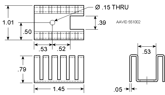
| 551002 | 0.59 | 0.79 | 1.01 | 1.45 | 16 | Screw on | 4.78 | 2.40 | 1.10 |
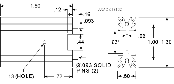
| 513102 | 0.97 | 1.50 | 1.38 | 0.50 | 15 | Screw on | 5.05 | 2.49 | 1.20 |
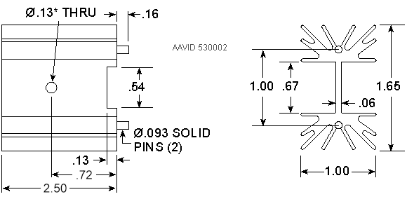
| 530002 | 1.58 | 2.50 | 1.65 | 1.00 | 7 | Screw on | 7.46 | 3.82 | 3.50 |
| Infinite | 9999.99 | 999.99 | 999.99 | 999.99 | 0 | Screw on | 11.00 | 6.00 | N/A |
Notes:
* Always use the heatsink with a good thermally conductive insulator
like the Bergquist K10 series (link
to Bergquist) (Digikey and other places have them). Use insulating
bushings if the transistor hole is metal.
* If you use a mica insulator, use new thermal grease each time you replace it. Use just a little grease. The grease is supposed to be about 0.003 inch thick after the screw is tightened.* Always support the heatsink some how. Don't let the leads of the MJE350 support the heatsink unless it is a tiny heatsink. If you bend the leads of the transistor too many times (sometimes as few as three times) the leads will break.
* If you use a film insulator (like the K10) or a rubber insulator, you should replace the insulator after every use. These insulators get their good performance by "cold flowing" to conform to the surface roughness of the transistor and the heatsink. Once they have been compressed, they won't conform as well on the next use. If you are not pushing the temperature rise (your decision, not mine) these could be re-used. I do not have numbers on how much worse they get with each use.
By double insulate I mean to put one insulator between the heatsink and the MJExxx. Find a different way to add more insulation around the actual heatsink and MJExxx. Such as attaching the heatsink to chassis with insulators and putting a safety cage around the heatsink so no one can touch it. One builder put a resistor and a neon bulb from the heatsink to signal ground so when the first insulator failed, the bulb lit up.* Put the heatsink where there is zero chance of anyone or anything touching it while power is applied.Watch out for stay capacitance if you attach the heatsink to chassis ground. This stray capacitance can make nasty high frequency ground loops. If you attach the MJExxx heatsink to chassis, make sure there is a ceramic or high frequency film cap from B+ to chassis right at the C4S to keep the high frequency ground loop small and thus not a problem..
Mark the heatsink as high voltage some how. People tend to think transistors only have 5V on them, not 500 V.
* The 150 C junction watts was found by solving:Watts = 1/( [10 C/W Rjs]/ 60 C rise + [C/W at watts used]/ 60 C rise)
You iterate on the "C/W at watts used" till you are happy with the accuracy or get irritated with iterating.
The 60 C rise is from 100 C junction - 40 C ambient temperature.
* The 10 C/W Rjs (junction to sink) is from 6.25 C/W Rjc (junction to case) + 3.75 C/W Rcs (case to sink).Watts = 1/( [10 C/W Rjs]/ 110 C rise + [C/W at watts used]/ 110 C rise)
You iterate on the "C/W at watts used" till you are happy with the accuracy or get irritated with iterating.
The 110 C rise is from 150 C junction - 40 C ambient temperature.
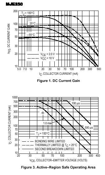
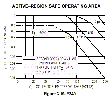
Take a look at the SOA of the MJE350. At 300V DC across the part, the transistor can only support 10 mA.
SOA Issues with the Transistor.
First Edition 02/10/01 Last Update 02/18/01
We need to check for this 300V 10 mA condition during worst case circuit conditions, not just normal operating conditions.
Things will break if the SOA is exceeded in any circuit, even in a current source. This means if the tube is shorted and the power supply at high line, we have to keep the voltage across the MJE350 below 300V and the current below 10 mA under this condition. Remember, silicon does not have a sense of humor. Don't mess with it's voltage ratings! I have found that when experienced designers I know say "they are pushing a transistor a bit", they mean they are starting to get close to the manufacture's ratings.
Think about this: SOA is also an accumulative failure mechanism. You exceed it by a little bit the first couple times, the part may not fail, but it degrades. Then when you are showing it off to friends, WHAM the darn thing fails.
This 10 mA at 300V should have some margin (also known as "pad", "derating" and "CYA".) Lets use 75% (3/4) and try to keep the 300V current below 7.5 mA. So if we use the MJE350 with a 300V supply, we need to keep the current through the MJE350 below 7.5 mA when it has 300V across it. If we need 8.0 mA, we'll use 8 mA. If we need 10.1 mA at 300V, we don't even think about it.
 (Curves
from www.OnSemi.com web site.)
(Curves
from www.OnSemi.com web site.)
A short table of the SOA MJE350 values.
"Power at 3/4 Pad" is the voltage times the 3/4 pad current.
| Voltage | Allowed | 3/4 Pad | Power at
3/4 Pad |
| 300 | 10 mA | 7.5 mA | 2.25 W |
| 200 | 25 mA | 18.8 mA | 3.76 W |
| 150 | 40 mA | 30 mA | 4.50 W |
| 100 | 95 mA | 71 mA | 7.10 W |
| 70 | 200 mA | 150 mA | 10.5 W |
 (Curves from www.OnSemi.com
web site.)
(Curves from www.OnSemi.com
web site.)
A short table of the SOA MJE340 values.
"Power at 3/4 Pad" is the voltage times the 3/4 pad current.
| Voltage | Allowed | 3/4 Pad | Power at
3/4 Pad |
Notes on
watts |
| 300 | 10 mA | 7.5 mA | 2.25 W | Can do |
| 200 | 28 mA | 21 mA | 4.20 W | Hot |
| 150 | 48 mA | 36 mA | 5.40 W | Good luck |
| 100 | 130 mA | 97 mA | 9.75 W | No way |
| 70 | 280 mA | 210 mA | 14.7 W | No way |
While we are looking at the curves, notice that the typical MJE350 25 C gain starts to drop at 70 mA. From the DC current gain curve (hfe), the typical gain is 90 at 50 mA. For both the MJE350 and MJE340 the minimum current gain is 30 at 50 mA from the data sheets. This is a 3:1 variation in nominal to minimum in the down direction only, the gain can go up too. Now you can start to see why I say the Pspice model only tells you what the model does and not always what the circuit does. Pspice uses the nominal gain, not the worst case gain. I like using Pspice; however, we should try to realize its limitations when we use it. We will checking these current gain issues out again later.
What happens when the SOA is exceeded? The transistor will have localized damage to the silicon. As this damage accumulates the transistor will perform worse and worse and all of a sudden the transistor will fail short. When this happens, the "R" of the CRC power supply and the cathode bias resistor in the tube could make a lot of smoke and possibly flame. If the tube was not damage before the transistor failed short, it probably is damaged after the transistor failed short. Don't mess with SOA or voltage stress on silicon, you will eventually and always lose. Messing with the SOA and voltage ratings of silicon is one of the things that gave solid state a bad reputation.
*** Also, do not reverse bias the base-emitter junction more than 3.0V. This will damage the junction, lower the DC gain and make the transistor noisy. If there is a chance of reverse biasing the base-emitter junction, put a diode across it to protect it. Remember that at power down, the coupling capacitor on the plate of a C4S fed tube discharges back through the C4S!
Limiting the voltage on the output of the C4S, the bad news:
Fixing a SOA issue: Limit the voltage before or after the C4S?
First Edition 02/10/01 Last Update 02/10/01
1. Limiting the voltage on the output of the C4S means you cannot use the C4S with a turn-on delay or LED ripple filtering. If you use a turn on delay you won't get the voltage drop across the output resistor that is used to keep the voltage across the C4S below 300V.Limiting the voltage on the output of the C4S, the good news:There are timing tricks to get around this problem. You make the time constant in the B+ much longer than the time constant in the C4S turn on delay/LED ripple filter.
1. Limiting the voltage on the output of the C4S this means when you run out of voltage swing, you do not hard clip. When you run out of voltage swing you go from a >5 meg drive impedance down to value of the resistor in series with the output of the C4S.Limiting the voltage on the B+ of the C4S with a regulator, the bad news:
2. Putting a resistor in the output of the C4S helps protect the C4S from reverse bias.
3. Putting a resistor in the output of the C4S buffers the tube from the output capacitance of the C4S.
1. You lose the benefits from having the resistor on the output of the C4S. (So put a 1K in the C4S output and get most of the benefits.)Limiting the voltage on the B+ of the C4S with a regulator, the good news:
2. You need to design a regulator.
1. You get extra noise filtering for the C4S. (You can almost never get enough noise filtering.)How about using a little of both methods!
2. It is easier to push the C4S near it limits and still sleep well at night.
3. You don't really need LED filtering anymore at low output currents (~ 1 mA).
4. This is usually compatible with a delayed turn-on of the C4S.
Even if it is just an extra RC in the B+.
Even when B+ is below 300V!
As I noted above while we are looking at the curves, notice that the typical 25 C gain starts to drop at 70 mA. From the curve, the typical gain is 90 at 50 mA. From the data sheet, the minimum gain is 30 at 50 mA. We need to know this minimum gain.Gain Issues with the Transistor.
First Edition 02/10/01 Last Update 02/10/01
Why do we care?
We need it to set the LED bias in the C4S.
The C4S LED bias is:
I bias =
LED bias currentWe will have to check bias current this later when we set the C4S resistor values.
+ I out maximum/30 for the cascode MJExxx transistor
+ I out maximum/60 for the current drive transistor. (The 2n2907A has a minimum gain of 60.)
How much B+ do we need to run a Constant Current Source (CCS) on a tube? An choke fed output tube can swing above B+ to make output power. A CCS can not. So we have to plan for a higher B+ to bias a tube with a CCS. Also, we should plan on having the plate to cathode voltage of the output tube move about 10% because the plate is current fed instead of voltage fed when determining the bias point.
Version 1 (my favorite)
B+ = ( 115 V AC/ 104 V AC ) * [ V_cathode_bias + V_plate_to_cathode
+ I_bias * R_plate_load + Plate_margin + CCS margin]
Version 2
B+ = ( 115 V AC/ 104 V AC ) * [ V_cathode_bias + V_plate_to_cathode
+ Max_V_swing + Plate_margin + CCS margin]
Note: Max_V_swing is the voltage swing from the plate curves between the bias point and the plate voltage with zero volts on the grid.
The standard Bottlehead C4S hard clips at about 3V across it. I've been playing with the MJE3xx models and curves. I've noticed that the (each) MJE3xx likes to see 10-20V instantaneous minimum across it instead of just 3V.
For an example, I'm going to use a 2A3 at 50 mA with about 15W plate dissipation feeding a 5K load. This CCS has three series pairs MJE3xx transistors (6 total MJE3xx devices).
Version 1
B+ = ( 110 %) * [ 60V + 310V + 50 mA * 5K + 10% of 310V for plate margin
+ 3 * 15V CCS margin ]
B+ = ( 110 %) * [ 60V + 310V + 250 V + 31V + 45V ]
B+ = ( 110 %) * [ 696 V ] = 766 V B+
Version 2
B+ = ( 110 % ) * [ 60V + 310V + (310V - 80V) + 31V plate margin
+ 3 * 15V CCS margin]
B+ = ( 110 % ) * [ 60V + 310V + 230 V + 31V + 45 V]
B+ = ( 110 % ) * [ 676 V ] = 744 V B+
If we were building a standard Parafeed, B+ would have been about 382V. (60 V cathode + 310 V plate to cathode + 12 V drop in the choke)
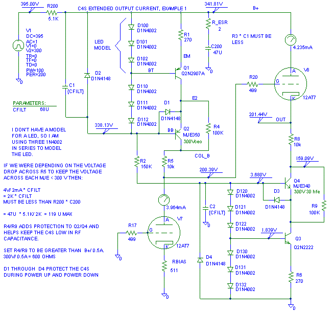
Playing with a C4S at 300V and 4 mA.
Not tried yet, remember I build
my own custom current sources.
First Edition 02/10/01 Last Update
02/22/01
Lets take a case where we want to drive 4 mA into a 12AT7 used as a cathode follower that is attached to a plate of a 12AT7 used as normal gain stage. Both are biased at 4 mA. The high line (26 mA load) B+ is 440V and drops to 395V under 60 mA load. The typical loaded B+ voltage is 360 V and the tube is at 170 V.
Tube use trivia: If we look at the curves for a 12AT7 at 4 mA, with zero volts grid to cathode there is 50V across the tube at 4 mA. This means that when driving low (towards ground), we run out of voltage swing at 50V in the gain stage and when driving high we run out of voltage at B+ - 50V in the cathode follower stage..
The C4S needs about 3V across it to function so if we were going to put a resistor in the output of the C4S it should be:
(50 V - 3 V)/4 mA = 37 V/ 4 mA = 11.75K (use a 10 K for 40 V drop)The C4S will have:
(360 V - 40 V - 170 V) * 4 mA = 150 V * 4 mA = 0.6 W across it at all times.This is OK if you don't mind a really hot part in your design.
Under fault conditions:
(340 V - 40 V) * 4 mA = 1.2 W (1.3 W = 150 C junction in a 40 C ambient.)This again is OK, but is marginal. To keep in the spirit of this page, I'm going to add a resistor to the C4S to reduce the power dissipation in the C4S. At 300V we would like the C4S to handle 20 to 25% of the current so that the current source operates nicely. If we put 3 mA (75%) into a parallel resistor, the C4S will be handling 1 mA (25%). Because this resistor is from collector to base of the cascode transistor, it does not drastically change the output impedance of the C4S.
300V/3 mA = 100K. 300 V^2/ 100K = 0.9WThe LEDs will need the following bias current:
(use a 2W for power and voltage reasons. Also note that most 2W are good for >350V)Maximum loss in the MJE350 will occur at 0.5 * I_out * R_parallel volts.
This loss will be ( I_out/ 2 )^2 * R_parallel. (I'll show the derivation for this later this year.)0.5 * 4 mA * 100K = 200 V across the MJExxx
( 4 mA/ 2 )^2 * 100K = 0.4 W
This is too hot to touch, but is cool enough to survive for a long long time.
2 mA (LED) + 4 mA/30 min gain MJE350 + 4 mA/60 min gain 2N2907A = 2.2 mA LED biasNow let's Zener regulate the B+ to 340V peak. This use a string of 1.5kexxxA zeners in series for the zener shunt. Knowing that the zeners will be +/- 5%, the minimum voltage for the zeners will be 340V * 0.95/ 1.05 = 307 V.
340 V - "3.3 V VA LEDs" - "3.3 V CF LEDs" = 333 V
333 V/ 2.2 mA =151 k (150 k 2 W)
333 V^2/ 150K = 0.74 W (use a 2 W)
It would be wise to skip reading this next section now and go look at the schematic below.
After you read the schematic, read these notes about a "failed" zener shunt regulator design if you are curious.
We will need a capacitor across the zeners to shunt the zener noise away from our circuit.
Circuit Hints: Zeners above about 6.8V are very noisy. Zeners below 5V don't regulate well.I will be happy if this zener shunt successfully operates as a zener clipper instead of a true shunt regulator. Generally, the voltage a zener regulator runs off of needs to be 50% higher than the output voltage + about 2 times the input voltage minimum to maximum voltage swing to have a reasonable zener regulator design.
There is no power rating curve for these zeners when the leads are not attached to a printed wiring board copper plane. These 175 C rated zeners have a little less surface area than the MJE350 transistor so lets assume they are 100C/ W:
(175 C - 40 C)/ 100 C/ W = 135 C / 100 C/ W = 1.35 W transient in the zener.First Shunt Regulator Iteration:
If we assume that high line on the B+ (Paramour terminals 14 to 15) is 395V, we want to drop
395 V - 340 V = 55 V in a series resistor.This leaves:
360V typical - 55V drop = 305 V available in normal operating conditions.In normal operating conditions the current flowing through the series B+ resistor is 1 mA for the zener, 2.2 mA for the bias resistor and 8 mA for the C4S.
R = 55V/ (1 mA + 2.2 mA + 8 mA) = 55V/ 11.2 mA = 4911 K, use 5.1K between the B+ and zener stack.With a turn on surge of 440V and assuming 307V on the Zener
(440 V - 307 V)/ 5100 = 133 V/ 5100 = 26.1 mA into the zeners.We need a better zener regulator.
(26.1 mA - 2.2 mA bias resistor) * 307 V = 7.34 W in the zeners.
Note: The C4S may not be conducting so the zeners have to adsorb the C4S current too.
7.34 W/ 1.35 W = 5.4 zeners, round up to 6 zeners.
340V pk/ 6 = 56.6 V peak each zener.
A 1.5ke51A (from Digikey) is 48.5 to 53.6V each or 291 to 321.6 V total (306.3V nominal).
The temperature co-efficient for this zener is 0.102 %/ C.
A 175 C rise from 25 C gives a 150 C delta in temperature for 15.3 % rise in voltage.291.0 V * 115.3 % = 336 V
321.6 V * 115.3 % = 370 V. (A 48.4 V rise during the surge just due to junction heating.)370 V - 340 V = 30 V too high for our C4S.
Second Shunt Regulator Iteration:
Turn-on surge conditions:
(440 V - 291 V)/5100 = 149 V/ 5100 = 29 mA
(29 mA - 2.2 mA) * 291 V = 7.8 W in the zeners at low zener voltage, room temperature junction.The above calculations show that nominally, the zener stack will protect the C4S. Worst case it won't protect the C4S because of the temperature coefficient of the zeners. This is a lot of work and parts for just nominal protection. We can improve this by adding a transistor to provide a negative temperature coefficient, but that is a different and future web site.
149 V^2/ 5100 = 4.35 W (use at least a 5 W 5100 ohm resistor)(440 V - 322 V)/ 5100 = 118 V/ 5110 = 23.1 mA
(23.1 mA - 2.2 mA) * 322 V = 6.7 W in the zener stack at high zener voltage, room temperature junction.(440 V - 340 V)/ 5100 = 100 V/ 5100 = 19.6 mA (Warm zeners)
(19.6 mA - 2.2 mA) * 340 V = 5.9 W in the zener stack. ( 0.983 W/ zener)
[ ( 340 - 306.3 V)/ 306.3 V] / 0.102%/ C = 11.0%/ (0.102 %/ C) = 107.8 C rise
107.8 C rise/100 C/W = 1.078 W allowed nominally in each zener.
Normal operating high line:
(395 V - 291 V)/ 5100 = 104 V/ 5100 = 20.4 mAIf we increase the 10K in the output of the C4S to 18K we will be dropping 72 V across the resistor so that under worst case surge conditions the C4S is protected (300 V + 72 V = 372V which is less than 370 V during the surge). However, this limits our positive swing to be 291 V - 72 V = 219 V. We need 170V + 60 V = 230 V peak typically to get full power out of the 2A3.
(20.4 mA - 2.2 mA - 8 mA) * 291 V = 10.2 mA * 291 V = 2.97 W (good)
104 V^2/ 5100 = 2.12 W in resistor, a 4 to 5 W resistor will be fine.
We will soon find out that it takes less effort to get more voltage
out of the C4S than it does to make the zener regulator, that is why I
am not pursuing the shunt regulator any further.
Start reading again!
* The 270 ohm (R1) may not give exactly 4 mA in a real C4S due to differences between the model I am using and what real parts will do.
The Example Schematic 1
Using a resistor across the C4S
First Edition 02/10/01 Last Update 02/17/01
Why can we get away with adding a resistor in parallel with the cascode transistor? (The MJE3xx transistors.)
We can get away with this because internal to the transistor there is a parasitic resistor from collector to base. This resistor changes with output voltage and output current. This resistor is determined by the "Early Voltage" of the transistor. The "Early Voltage" is not specified in the transistor data sheets. Rats! :-(
If we put the transistor on a curve tracer, there will be a slope (resistance) to the output current as the output voltage is changed. If we extend these slopes to where they cross zero current, they all cross at nearly the same point. This point is a negative voltage for a NPN transistor (MJE340) and a positive voltage for a PNP transistor (MJE350). This point is called the "Early Voltage". The "Early Voltage" is usually expressed as a positive number and the engineer has to figure out what the polarity really is.
Now lets get even deeper in to the theory. (Break out the Aspirin.)
Second order, the current set transistor (2n2907/ 2n2222) sees two things that affect the output impedance, both are changes in voltage:
1. There are variations in the base current of the MJE350. These variations times the impedance of the LEDs will cause the voltage across the 2N2907A's collector to vary and will also cause the 2N2907A's base voltage to vary. The lower the impedance of the LED, the less effect the base current changes of the MJE350 will have on the output impedance. Keeping the LED impedance low is why you need a capacitor across the LEDs. In example 1 above, the second cap would go from BT to B+ to be across the top LED. 68 uF is the smallest I'd use. 1000 uF 6.3V caps are easy to find, so use them.
The variations in base current are from:
A. The the parallel resistor from emitter to collector of the MJE350 causing the collector current to change to change,2. There is a variation in base-emitter voltage of the MJE350 because the MJE350's collector current is changing. This change is 17 mV (25 mV in some books) change for a 2:1 collector current change. This voltage change and the "Early voltage" are two of the reasons I am recommending that the maximum ratio of transistor current to resistor current be 1:4 (20% MJE350 to 80% resistor) to keep the variation in the output impedance under control.
B. AC current flow from the miller capacitance and
C. Collector to base leakage current/leakage resistance.
Adding 6 zeners and still not getting good protection for the C4S is not my idea of a good investment. Especially since the zeners are not always forward biased so that they will give the benefit of DC filtering (attenuation of input ripple.)
If we did not use a shunt regulator, the 5.1K
resistor in B+ needs to only handle the C4S currents of 2.2 mA bias + 2
* 4 mA = 10.2 mA.
5.1K * 10.2 mA^2 = 0.53 W. The 5.1 K resistor
only needs to be a 1 W part.
Instead of adding a shunt regulator, let's extend the C4S's voltage rating. We will want to keep the B+ filtering mostly because of the cathode follower. I will only show the mod to the "VA" (Voltage amplifier) 's C4S. The "CF" (Cathode follower) 's C4S is modified in the same way but uses a MJE340 instead of a MJE350 and the diode across the base emitter gets reversed.
With two stacked transistors, the resistor in parallel with the MJE350s can significantly affect the output impedance. This usually only occurs with low amounts of voltage across the modified C4S. This occurs mostly because the added transistor stage can't get enough base bias current to operate correctly when there is little voltage across the C4S. We can correct this by making the parallel resistor smaller, but if we make it too small, performance may also suffer with lots of voltage across the C4S. Solving this problem is where Pspice and similar programs can help you out.
To get to 600V, the following parts are added: another MJE350, another 1n4148 protection diode and another 100K resistor. I am assuming the stock C4S already is modified with D1, D2, R4, R5 and C1. R4 is no longer attached to the collector of Q2 but to the base of Q3.
The 270 ohm (R1) may not give exactly 4 mA in a real C4S due to differences between the model I am using and what real parts will do.
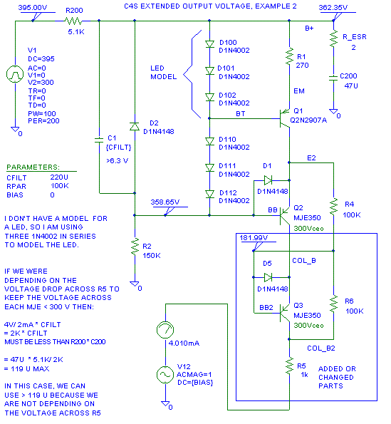
During normal operation there will be 200V maximum across R4 and R6. This is 0.4 W each so R4 and R6 could be 1 W resistors. Neither Q2 nor Q3 needs a heatsink in this example. We don't need to clamp the B+ for turn-on surge either.
From the Pspice model, this modified C4S is good to about 15V drop across the C4S not counting the 4 V across R5. To add a "safety" margin to the calculated drop out voltage, I'd add a correction for the base current of Q3 into the two 100K resistors that drive Q3's base.
4 mA/30 * 1/(1/100k + 1/100k) = 0.13 mA * 50 K =
6.7 V.
15V + 4V + 6.7 V = 27V less then B+. We can live
with this much voltage drop.
We've already calculated the power loss in Q2 and Q3 for more voltage than they will ever see in a Paramour.
If we want to use this circuit at 600V, R2 becomes 270K >2 W (I'd use three 91 K 1 W in series for the 270 K) and R4 and R6 become 2 W each. With these changes the modified C4S will almost work to 600V peak B+. The "almost" is because Q2 and Q3 won't share voltage perfectly.
The maximum voltage across each MJE350 will be 300V. The 600V peak rating is so we can survive turn-on and line surges. The 300V across the MJE350 limits the current to be 7.5 mA so the collector to base resistor needs to conduct
(45 mA - 7.5 mA) = 37.5 mAThere should be a resistor in series with the C4S output to limit the current through the C4S to 0.5 A peak during power down or output faults:
R = 300V/ 37.5 mA = 8000 ohms
300 V^2 / 8000 = 11.25 W use at least a 15 W wire wound.
600 V/ 0.5 A = 1200 ohms (use 1.5 K)Maximum dissipation in the MJE350 occurs at:
45 mA * 1.5 k = 67.5 V drop
45 mA^2 * 1.5 k = 3.04 W loss. (Use three 2 W 510 ohm resistors in series for the 1.5 k)
Do you have to add these resistors?
No.
If you can't afford the 68 V drop. Try to use one 510 ohm resistor for a 22 V drop.
40 mA/2 * 8000 ohm = 160 V across each MJE350.This would occur with
(600 V B+) - (2 * 160 V per C4S) - (68 V for the series resistor) = 212 V on the plate of the tube.This power loss is:
(40 mA/ 2) ^2 * 8000 ohm = 3.20 W per MJE350 (We will need a heatsink.)For 100 C junction at 40 C ambient:
(100 C - 40 C)/ 3.2 W = 18.8 C/ W total heatsinkingDouble insulate this heatsink.
Heatsink needed = 18.8 C/W - 6.25 C/ W transistor - 3.75 C/ W Bergquist K10 insulator
= 8.75 C/ W actual heatsink needed per MJE350 at 3.2 W loss each.
(A lower C/ W is even better.)
Insulate from the transistor to the heatsink.Because maximum power loss in the MJE350's occurs near normal operating conditions, the power loss in the MJE350 will be less when the tube is shorted than in normal operation. This means we don't have to calculate the 150 C junction conditions. Into a shorted tube:
Insulate from the heatsink to chassis and signal ground.
Finally put the heatsink where there is zero chance of anyone or anything touching it while power is applied.
(600 V - 68 V) * (45 mA - (600V - 68V)/16000 ohm)/ 2 transistors =We need to check the SOA at several points:
532 * ( 45 mA - 33.25 mA)/ 2 parts = 6.25 / 2 parts = 3.13 W each transistor.
| MJE350
Voltage |
Resistor
mA |
Actual
MJE350 mA |
Allowed
MJE350 mA |
Ok or not |
| 300 | 37.5 | 7.5 | 10 | OK |
| 250 | 31.2 | 13.8 | 17 | OK |
| 200 | 25.0 | 20.0 | 25 | OK |
| 150 | 18.7 | 26.3 | 40 | OK |
The LED bias will be
2 mA + 45 mA/30 + 45 mA/60 = 4.25 mAThese three resistors can be used as a balancing network to stack three > 200V capacitors to make a 600V B+ filter capacitor that the C4S runs from. I drew this using three capacitors to illustrate how to stack multiple capacitors and provide bias for the C4S at the same time. C201 to C203 are just values pulled out of a hat. If you use just one cap on B+, R5, R6 and R7 are still needed to bias the C4S.
600 V/ 4.25 mA = 141K.
600 V^2/ 141K = 2.55W. Use three 47 K 2 W in series for 141k 6 W
Please use a reasonable amount of capacitance from B+ to ground. 470 uF/ 3 is on the high side of what you'll want. As a WAG, 1 uF is on the low side of what you want.
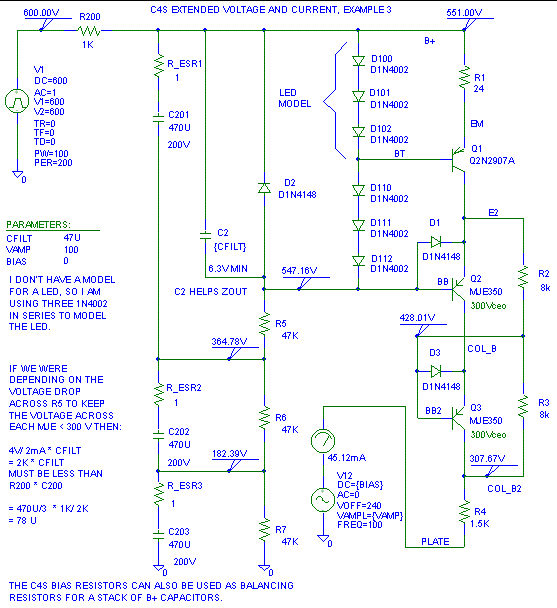
Theoretical Performance Plots of Example 3
Last update 02/18/01
PSpice does not know about SOA. It will let
you put 2 kW into a 1/4 W part. PSpice will tell you what the parts do
at the temperature you select. The thermal analysis is up to you. (PSpice
does know about breakdown voltage on most parts.)
Lets look at the output impedance of the above circuit with the "tube" voltage at ground (0V) up to 500V. By varying the DC voltage of V12, I can simulate different bias points on a tube that is being fed by the current source. From the curves, this circuit needs 100 V across it to function. Of these 100V, 68 V is lost across R4, the protection resistor.
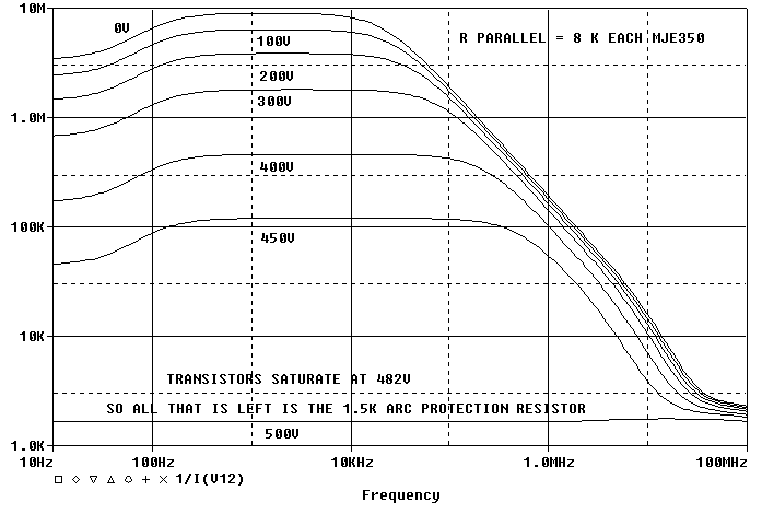
First lets check the variation in Z_out with load voltage with R2 and R3 = 8K. The voltages listed on the plot are the plate voltages of the tube:
Now lets check it with R2 and R3 = 51K each.
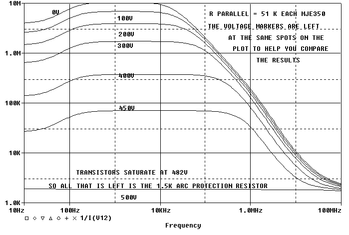
If R2 and R3 are the major sources of the variation, we should see a huge change in Z_out. I'm seeing some variation, but not a huge variation. Between 0 and 200V the 51K version looks like it works better. Between 300 and 450V the 8 K version seems to work better.
To handle the same SOA as the 8 K parallel version, we would have to have 5 sets of 51K parallel version to get the same SOA. This would drop the output impedances by 5. The 8K to 51K variation in Z_out is much less than 5:1.
Now lets check the curve out with and without C1, the LED bypass capacitor.
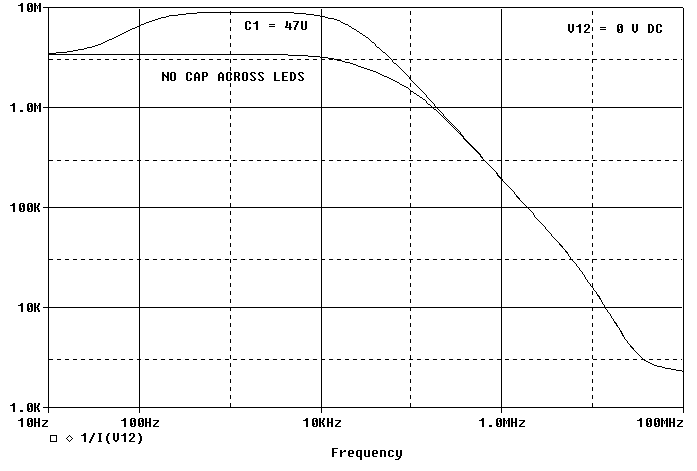
The LED bypass capacitor is worth having. The LED bypass capacitor also improves the power supply ripple rejection.
With R2 and R3 = 8K, here is the calculated distortion. It looks bad but it isn't!
400V pp is nearly full output swing.
10 uA of distortion (20 uA pp) being fed into a 600 ohm plate only
makes 12 mV pp of distortion. Referencing this to 400 V pp, the 4th harmonic
is about 90 dB down. As we back off from 400 V pp, things get better fast.
At 200 V pp third harmonic (300 Hz):
~1 uA peak (~2 uA pp) * 600 ohms = ~1.2 mV pp.
20 log (1.2 mV/ 200 V) = -104 dB. Better than a CD player can hope for.
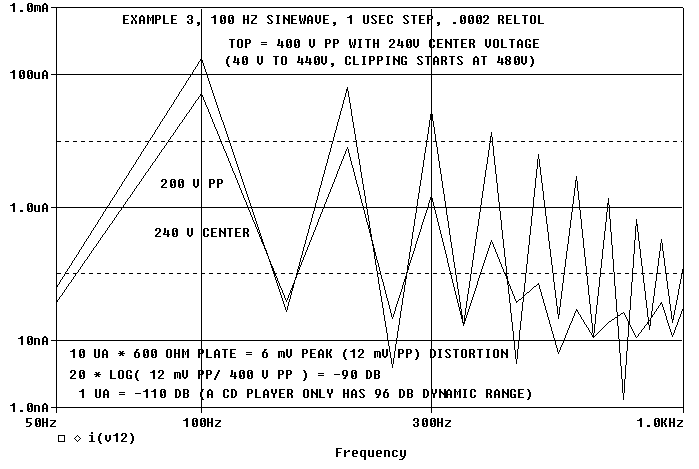
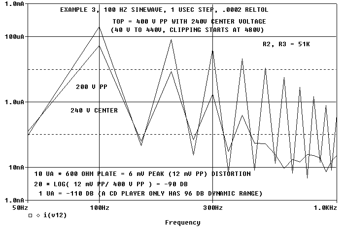
The 8K distortion actually looks better than the 51K distortion. Please keep in mind that these plots are for a distortion less tube and with the part model I got from the MJE350's vendor web site. As we are fond of saying: Your mileage may vary (YMMV).
I have omitted any bonus voltage from the tube's cathode resistor in
the above discussion. I did that to avoid making this topic even more complicated.
If you have a 1000 uF bypass capacitor on your cathode resistor, you don't
get any bonus points during tube arcs during power up any way.
Malcolm Hawksford, "Reduction of Transistor Slope Impedance Dependent Distortion in Large-Signal Amplifiers", J. Audio Eng. Soc., Vol. 36, No 4, 1988 April.
The trick shown in Hawksford article has wonderful performance below
100 kHz. Pspice modeling indicates that it had a lot of RF gain and if
you are not careful, it can ring or oscillate in the 10 to 100 MHz region.
Why do you care about the 10 to 100 MHz region? Because if a parasitic
oscillation causes the current source to clip or go non linear at RF frequencies,
it will cause distortion at audio frequencies.