Cascading the C4S in the
B+ for higher PSRR
Power Supply Rejection Ratio is how good a circuit
rejects power supply noise.
I am posting this to help out a few "advanced
builder" friends, you've got to do you own math to make this work.
I'm not sure if I like this idea yet. It looks
good on paper so far, but it does not" feel" right.
These circuits involve high voltage. Try them
at your own risk!
The C4S stands for "Camille Cascode Constant Current
Source." It was designed by Buddha (John Camille). This current source
is simple, robust and in my opinion functions very well. Bottlehead sells
the basic C4S as a kit.
I had a friend ask how to cascade two C4S in a
power supply so that he could get more power supply rejection. He said
that Budda had mentioned that this could be done. You would start with
the raw B+ and have a C4S feed a capacitor. This capacitor feeds the C4S
that runs the output stage. This can get you a lot of attenuation in a
very small space as opposed to cascading RCRCRC stages or LCLC stages.
The problem with implementing this with a standard
C4S is mostly with the variation in current in the C4S. The C4S changes
in current because of value/gain changes in the parts, changes in
current over temperature and changes over time (mostly the LED).
The problem:
If the first (top) C4S drifts up in current,
it will pull the capacitor it feeds up in voltage until the first C4S saturates
and now all the benefits of the top C4S are lost.
If the first (top) C4S drifts down in current,
the voltage on the feed capacitor will start to drop and the output stage
will clip on loud passages or stop to work entirely.
To reduce this sensitivity, I made a few changes
to the top C4S circuit.
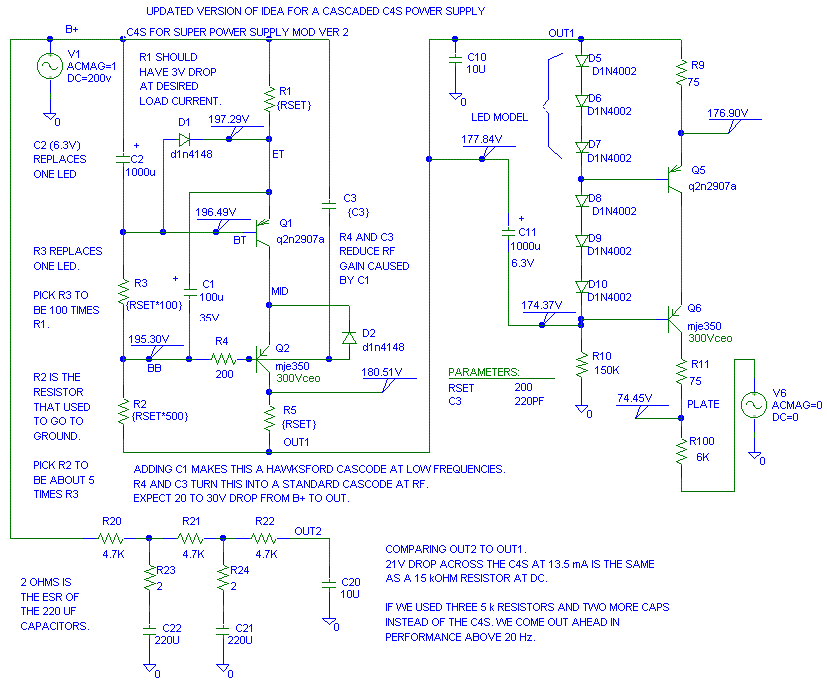
This is basically how the C4S gets set up:
"OUT1" is the high volts that feeds the final
C4S.
"OUT2" is a reference RCRCRC filter stage with
the same voltage drop as the modified C4S.
"PLATE" what the voltage on a 6K plate of a tube
will look like for a given B+ ripple.

Notice that I have my normal protection resistor in the collector of
Q2 and Q6. A good value for this resistor is to use the same value as you
are using for R1 or to use R = B+/ 0.5 A. I used a 1N4148 for the base
emitter protection resistor. A UF1007 is a better choice, but I don't have
a model for that (yet.)
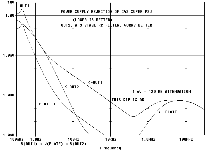
Here is what the different voltages look like with 1V of ripple on B+.
Notice that the RCRCRC stage actually works better.
I'd guess the RCRCRC version would occupy 3 times the volume as the
C4S version.

The OUT1 peak at 0.2 Hz worries me. This peak could mean that
there is a sensitivity to low frequency noise. I don't fully understand
the OUT1 peak, but I have only spent enough time to throw together a simple
model.
I am also showing a Hawksford Cascode connected C4S in the schematic!
The Hawksford Cascode has a capacitor or a zener between the
emitter of the current set transistor to the base of the cascoding transistor.
This way of making a cascode has more feedback than a standard cascode.
The feedback is from the base of the cascode transistor to the emitter
of the transistor that attaches to the current set resistor. This feedback
feeds the current from the collector to base capacitance of the cascode
back to the local feedback point (the emitter of the current set resistor.)
Because of this feedback, the output impedance is greatly increased
and the output distortion is reduced.
Unfortunately, this extra feedback can make
the Hawksford Cascode ring at RF frequencies. I added a resistor and a
capacitor (C3) to turn the Hawksford Cascode back into a standard cascode
at RF frequencies so we get our stability back. The added capacitor (C3)
should be a mica or ceramic with very short leads, do not use a metalized
film.
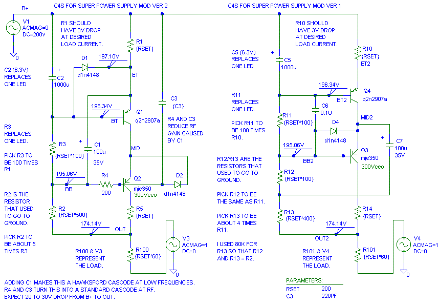
Lets compare the two versions (Hawksford vs non-Hasksford) of this modified
C4S:

Notice that I have my normal protection resistor in the collector of
Q2 and Q3. A good value is to use the same value as you are using for R1
or to use R = B+ / 0.5 A.
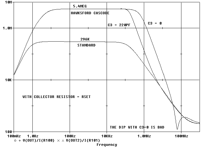
If we remove C3, we see a nasty notch in the output impedance of the
modified C4S. It is very easy for this notch to get out of control if we
leave out C3 and R4
Notice look at the improved output impedance in the audio band and
out to 100 kHz. A full 25 dB of improvement.

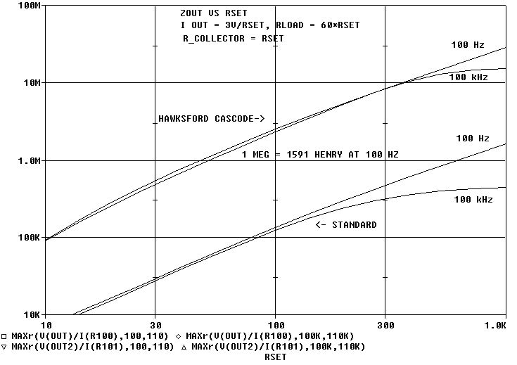
In the plot below, I kept C3 and R4 the same (220 pF and 200 ohms) and
swept the load current and associated resistor values in the modified C4S.
The Hawksford version of the C4S works much better.

With all said and done, I would personally use the RCRCRC filtering
if I could afford the space needed for the extra resistors and capacitors.
The last C (the one that attaches to the tube) is the one that needs to
be the best quality. The first two Cs (220 uF) just need to have long life
and low ESR.
With RSET = about 50 ohms for 3V drop at 60 mA throughput and using
the Hawksford Cascode mod, the graph above says we should see about 1 megohm
at 100 Hz. To get 1 megohm at 100 Hz, we would need 1561 henries of inductance.
That's a big choke. This big choke will probably have more capacitance
at high frequencies than the C4S.
60 mA * 30V drop = 1.8 W, that is a do able heatsink size for a C4S.
Make sure you watch the SOA during power up. I did not draw the SOA curves
here. I learned about SOA the hard way using a current limited transistor
to charge up a capacitor. The transistor died about every 15 power ups.
The C4S approach should be smaller than the RCRCRC approach and does
show promise. There still are a few questions left to resolve about power
up and the low frequency peak.
A few ideas:
How about replacing the 270 ohm resistor in the Paramour with a C4S
that works like this!
I think I have a new mod to try after VSAC!
I may just make a version of the active filter already on may Paramour
page and just leave the delay out.
Adding a choke is much easier to do. Since when is the easy way the
fun way!
I Think I have Figured it
out.
This involves working with high voltages,
attempt this at your own risk.
Added 09/01/02 Updated 09/01/02
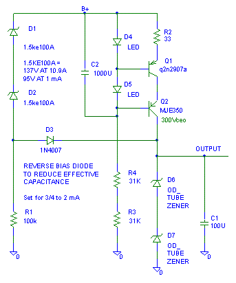
The problem with using the C4S in a power supply
near 300V is the turn on surge. When the C4S sees more than 300V, it will
be toast. When it fails, it will probably cause a few more parts to toast.
This example is for a shunt regulated supply:

D1 and D2 adsorb the turn-on surge between B+ and OUTPUT through D3.
Remember, C1 looks like a short at turn on.
With R1 to bias D1 and D2 on in normal operation, D3 should be reverse
biased isolating the output from the high capacitance of D1 and D2.
First edition 2-Sep-01, last update
09/10/01 I don't change the update date on individual sections for minor
corrections. I only change the date for content changes.

